
As semiconductor device feature sizes shrink and new nanoscale materials are developed, traditional characterization tools used to study local changes within semiconductors and electronic circuits start becoming obsolete. With in situ TEM, you can image systems at atomic resolution to conduct understand working conditions or test the performance of new devices and materials in your lab.
Fusion AX: Study high temperature heating, electrical and electrothermal in vacuum
Follow resistive switching processes, charge and discharge nanobatteries while measuring columbic efficiency, and study your materials’ electrical properties at high temperature, all without compromising on resolution.
Click here to learn more about our in situ heating and biasing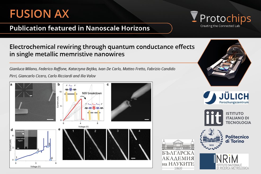
Featured Papers
-
News
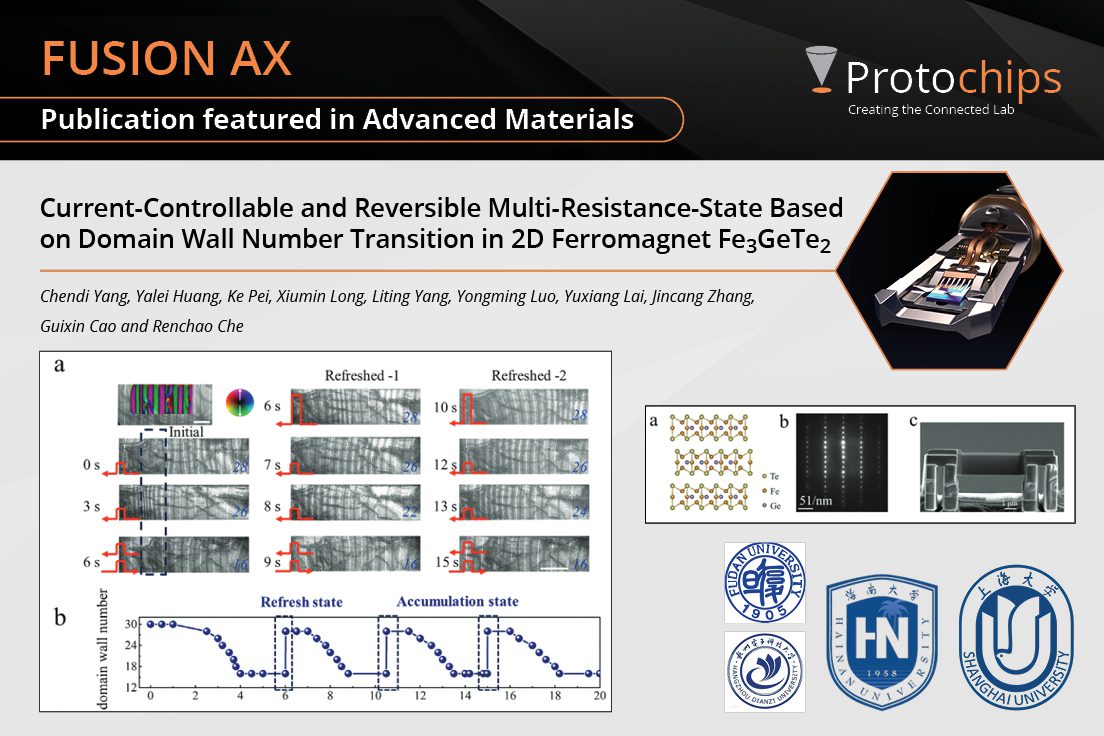
Current-Controllable and ...Jul. 9, 2024 -
News
Electrochemical rewiring ...Apr. 23, 2024 -
News
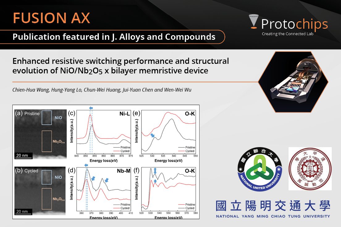
Enhanced resistive switch...Mar. 26, 2024 -
News
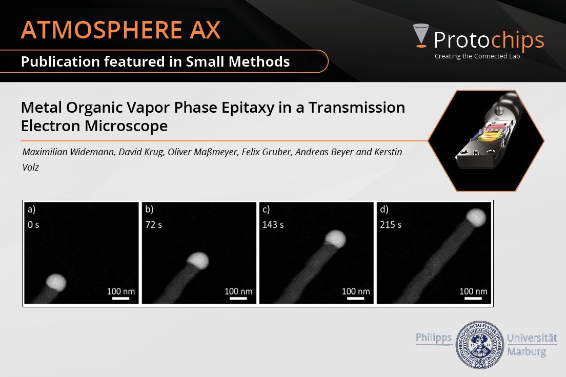
Metal Organic Vapor Phase...Feb. 12, 2024 -
News
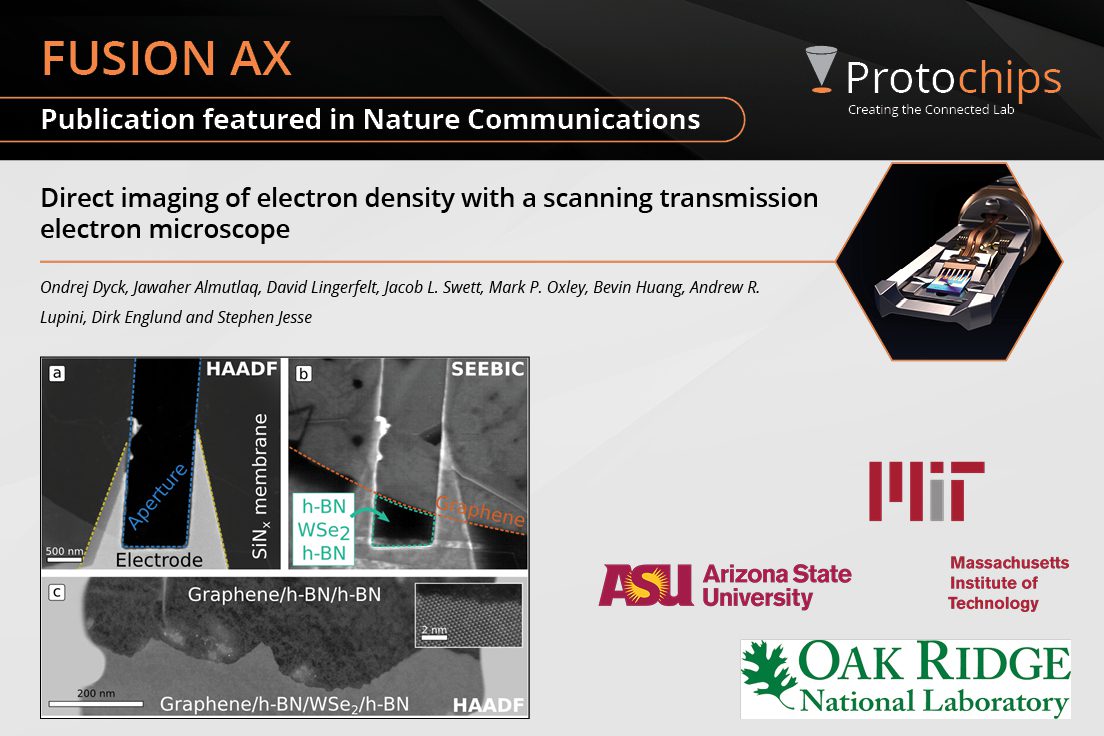
Direct imaging of electro...Feb. 6, 2024 -
News
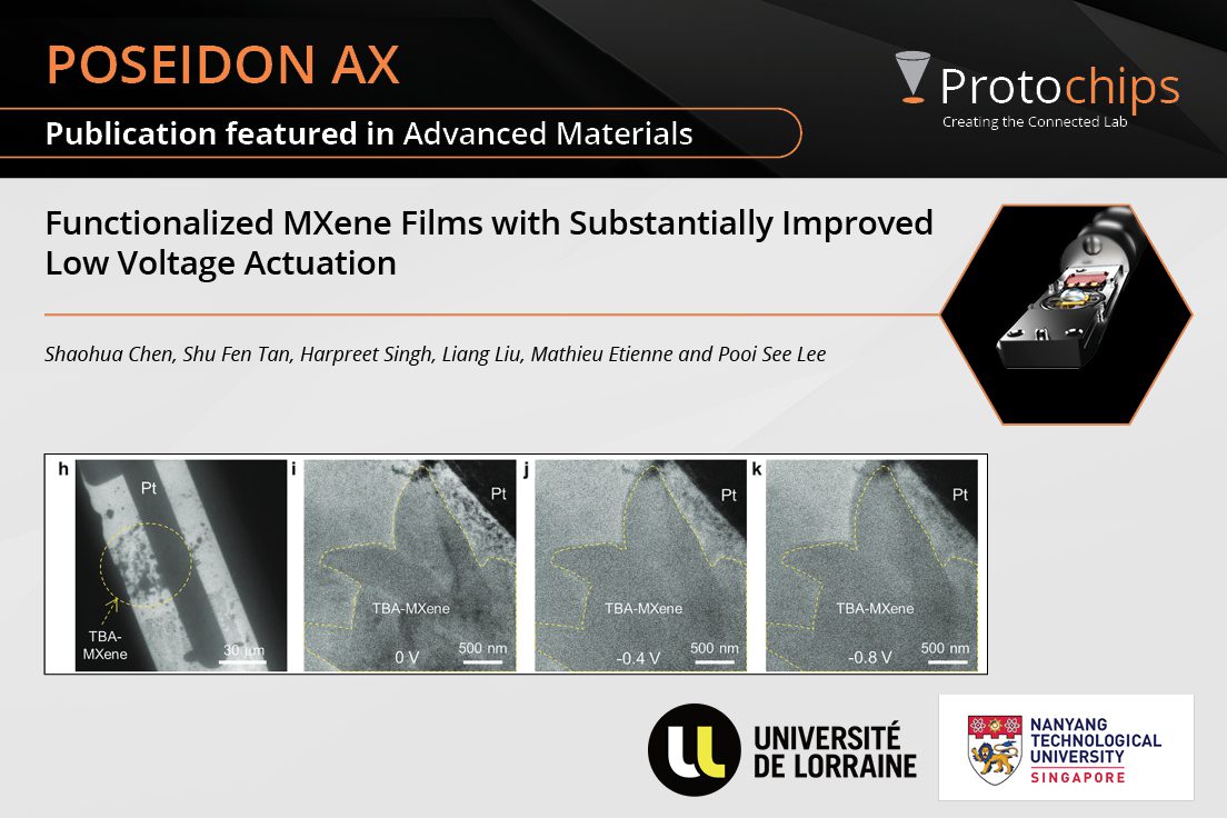
Functionalized MXene film...Jan. 30, 2024 -
News
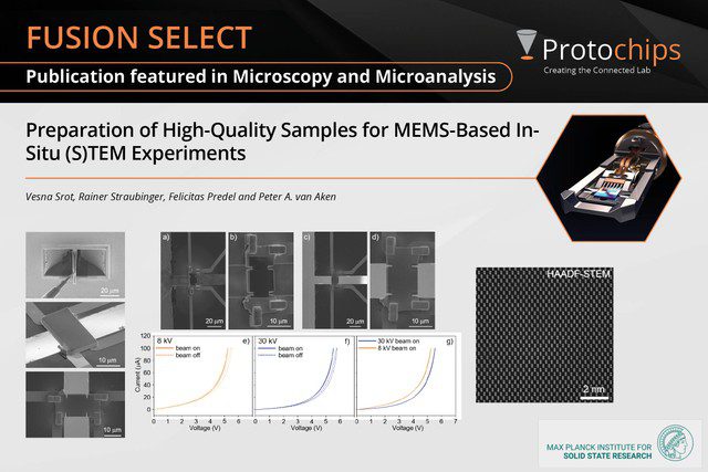
Preparation of High-Quali...Mar. 7, 2023 -
News
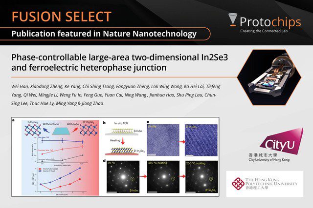
Phase-Controllable Large-...Jan. 24, 2023 -
News
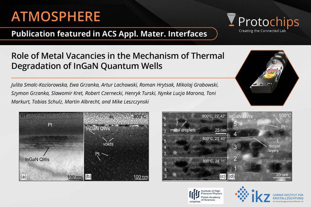
Role of Metal Vacancies i...Dec. 9, 2022 -
News
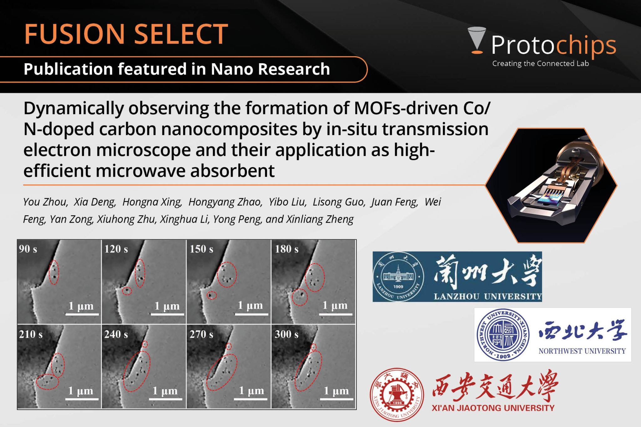
Dynamically observing the...Oct. 17, 2022
What have our users done in the field? Read our summaries here!
-

Electronic Devices One Pager
Download the one pager that shows how Poseidon AX can be used to study electronic devices with in situ electron microscopy.
-
Using Protochips AXON Software for Tracking Electron Flux and Cumulative Dose
In this paper, we take a look at how AXON Dose tracks the electron flux and cumulative dose, and why this might be useful for all experiments.
-
Simultaneous Electrical and Heating Using Fusion: Electric-Field Assisted Sintering of ZrO2 Nanoparticles
In this summarized paper, researchers in the van Benthem group at University of California, Davis, studied sintering mechanisms in 3mol% yttria-stablized ZrO2 (3YSZ) nanoparticles using Fusion system with electrical biasing capabilities.
-
Off-Axis Electron Holography Under High Temperature and Oxidizing Environment
In this paper, in situ heating and off-axis holography were combined to better understand the magnetic redistribution in magnetite particles. This work was conducted by multiple groups including Almeida at Imperial College London, Dunin-Borkowski at the Ernst Ruska-Centre for Microscopy and Spectroscopy with Electrons (ER-C) and the Peter Grünberg Institute and Hansen at Denmark Technical University (DTU) Center for Electron Microscopy.
-
In Situ Atomic Structure Manipulation of Graphene
In this summarized paper, Chen in the Zettl group at UC Berkeley and Lawrence Berkeley National Lab transferred single layer graphene to E-chips and made electrical contacts via electron beam lithography. Moreover, Qi in the Johnson group at Pennsylvania used the Fusion system to apply electrical current at slow voltage ramping rates.
-
Visualizing the Electrical Switching Mechanism in ZnO-Based ReRAM Devices
In this summarized paper researchers from National Chiao Tung University in Hsinchu, Taiwan used the Fusion system to perform electrical biasing on a thin sample from a ReRAM device, which consisted of a ZnO layer sandwiched between two Pt electrodes.
-
Atomic Scale Imaging of 2-D Materials
This paper shows how Alex Zettl’s lab at UC Berkeley and at the National Center for Electron Microscopy at Lawrence Berkeley National Laboratory (NCEM, LBNL) have characterized the atomic scale structure of CVD grown h-BN in situ in the TEM using a Fusion system
Videos
Watch dynamic behavior of real samples in situ.
Using the Protochips Fusion System in the SEM, we show Schott glass melting at ~620 °C. Its known melting point is 622 °C. This demonstrates the accuracy of the Fusion heating system. For more information on Fusion, visit www.protochips.com/fusion.
This video shows gold nanoparticles at 600 C. The video shows the stability of the Protochips Fusion™ at high temperatures and the ability to resolve dynamic events with sub-Angstrom resolution. The initial video was taken at 1 frame per second, and then sped up to 5 frames per second using video editing software later. The video was taken in the TEAM 0.5 microscope (FEI Titan, 300 kV, Cs aberration correction, monochromator) at Berkeley National Laboratory, Berkeley, California.
This workflow explains the procedure for preparing FIB samples onto a MEMS-based E-chip for in situ TEM. FIB sample preparation can be used to prepare a wide variety of materials for TEM or in situ TEM analysis and is a relatively simple technique to learn. For more information, tips and tricks, and sample preparation guides, visit our library of content at www.protochips.com