

In situ studies enable researchers to replicate a nanomaterial’s synthesis or operating conditions to uncover the fundamental pathways that control its growth, interactions, and stability. In the course of time, this will support the development of new, more efficient and safer nanomaterial technologies.
Poseidon AX: Liquid, electrochemical and liquid heating in situ studies
Image real time nanomaterial synthesis and nanoparticle interactions in liquid.
Click here to learn more about our liquid cell solution
Atmosphere AX: Gas and vapor high temperature environment
Image nanoparticle reduction, growth, oxidation and even corrosion studies under relevant temperatures, atmosphere and pressure.
Click here to learn more about our gas cell solution
Fusion AX: Study high temperature heating, electrical and electrothermal in vacuum
Heat particles to investigate nanoparticle formation while observing chemical and structural changes in situ.
Click here to learn more about our heating and biasing solution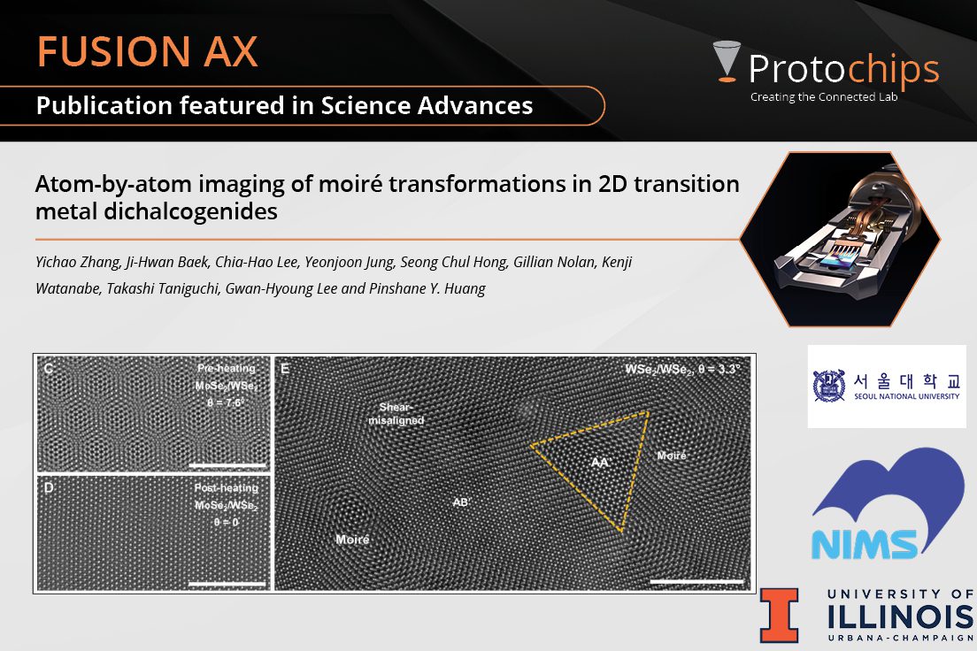

Featured Papers
-
News
Spontaneous Liquefaction ...Sep. 3, 2024 -
News
Atom-by-atom imaging of m...Jun. 25, 2024 -
News
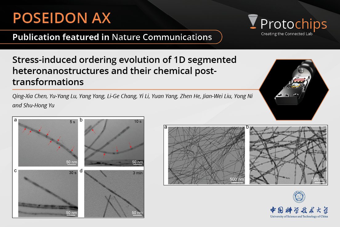
Stress-induced ordering e...May. 28, 2024 -
News
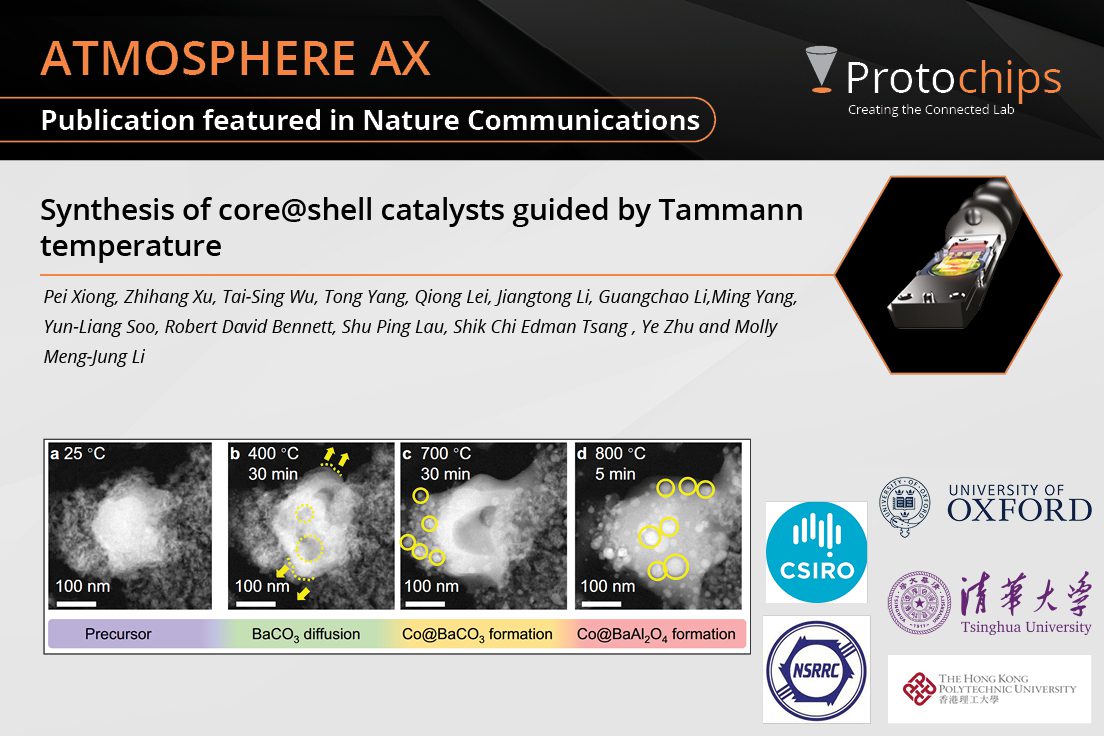
Synthesis of core@shell c...Mar. 5, 2024 -
News
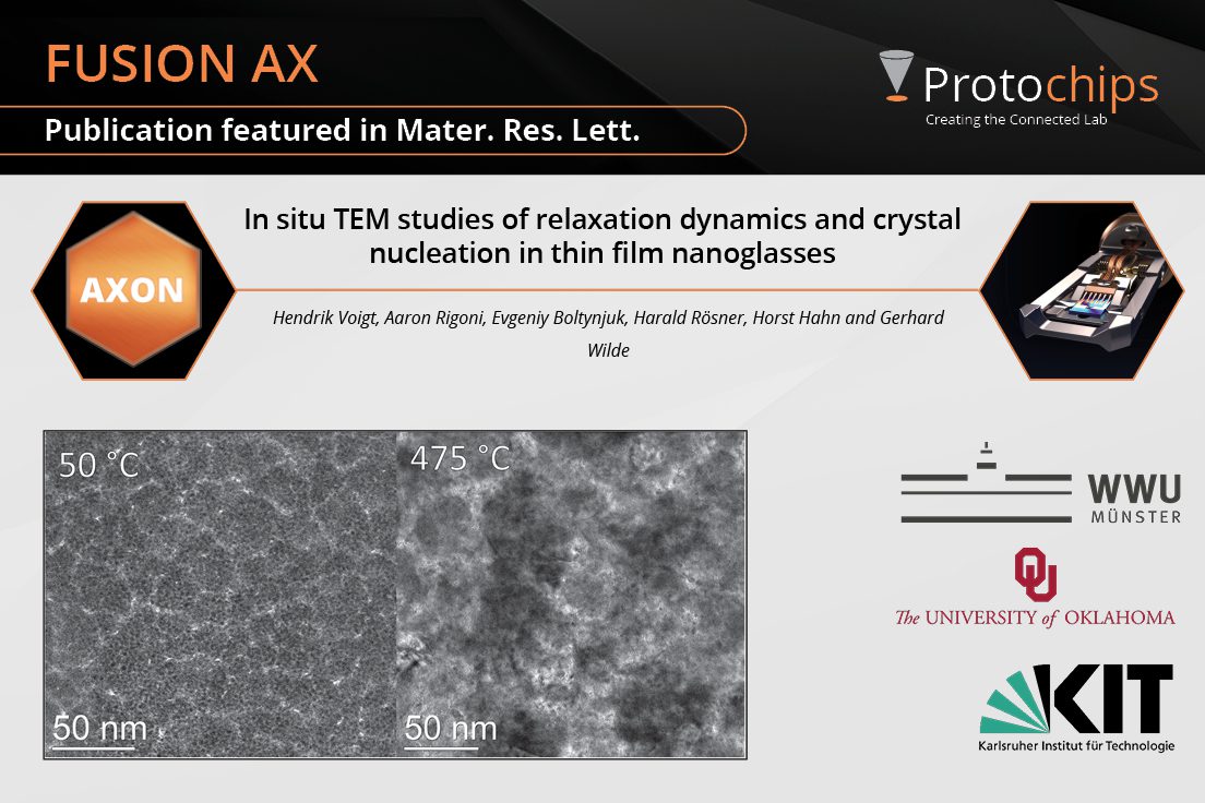
In situ TEM studies of re...Dec. 19, 2023 -
News
Unraveling and leveraging...Dec. 1, 2023 -
News
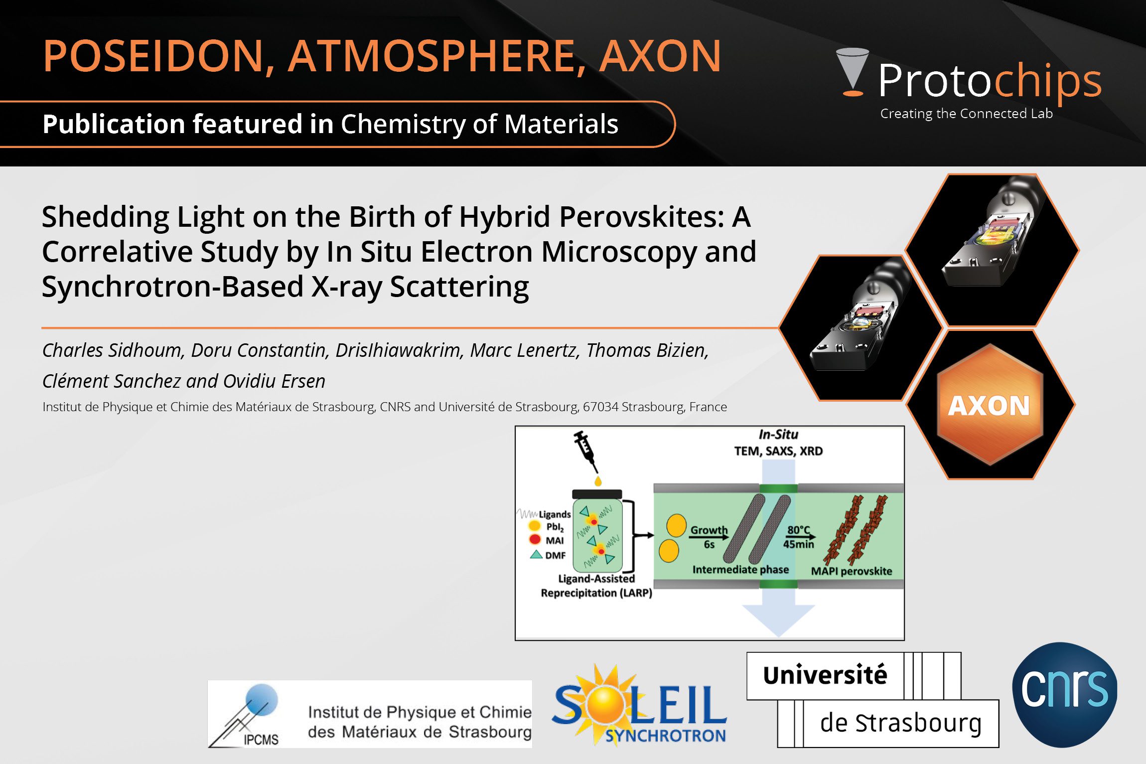
Shedding light on the bir...Nov. 17, 2023 -
News
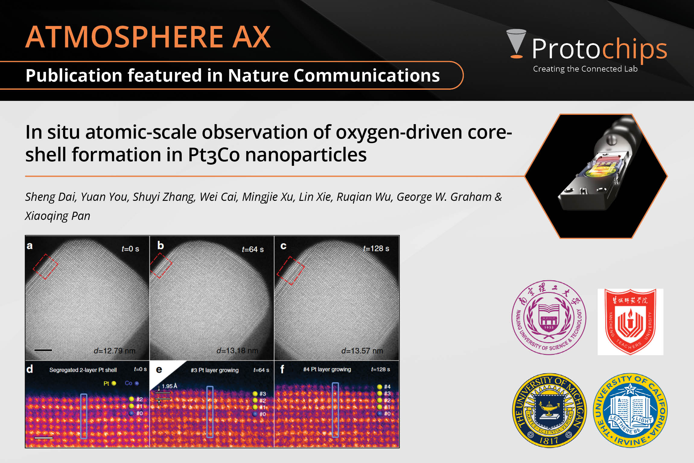
In situ atomic-scale obse...Oct. 31, 2023 -
News
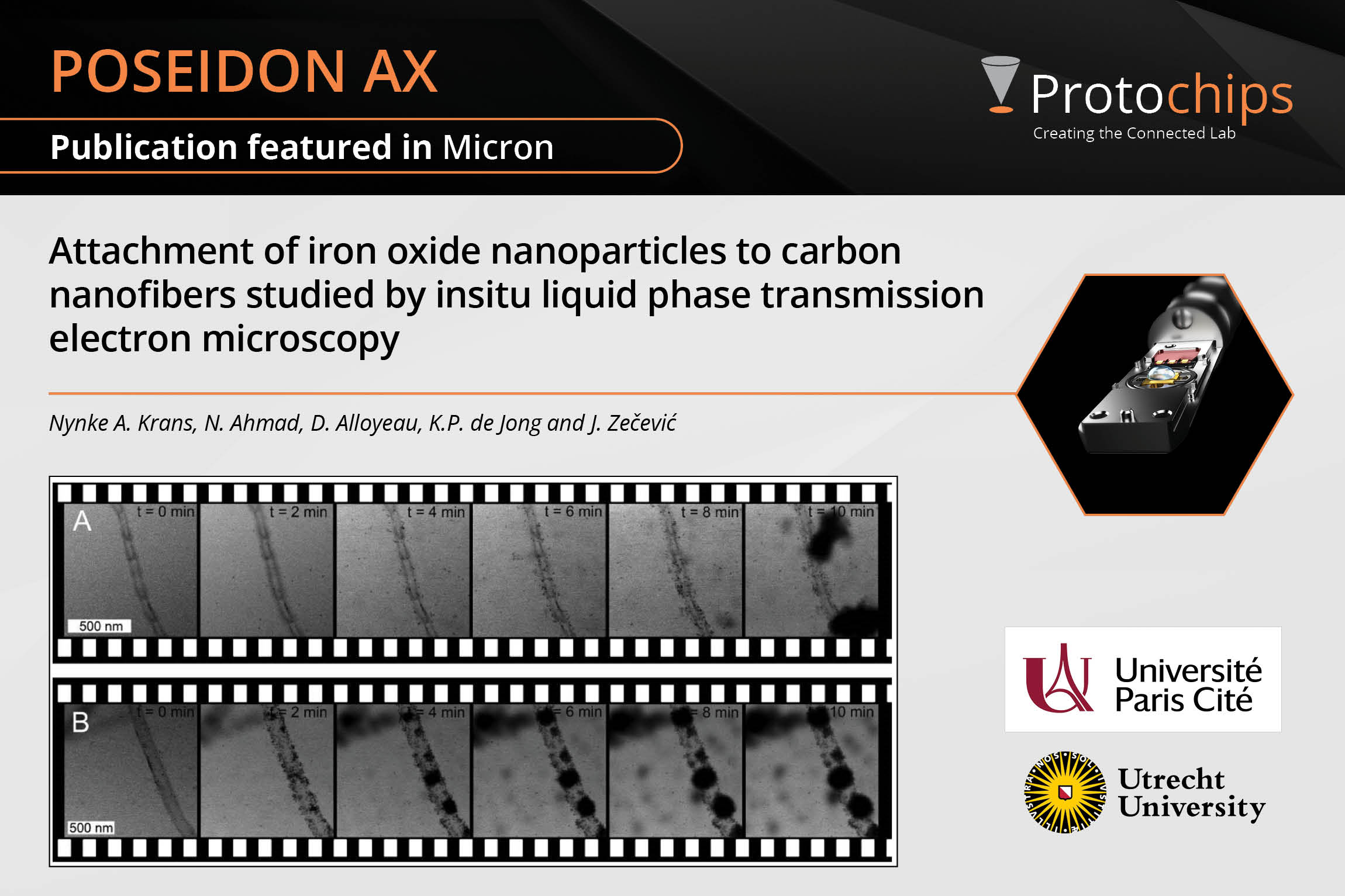
Attachment of iron oxide ...Aug. 22, 2023 -
News
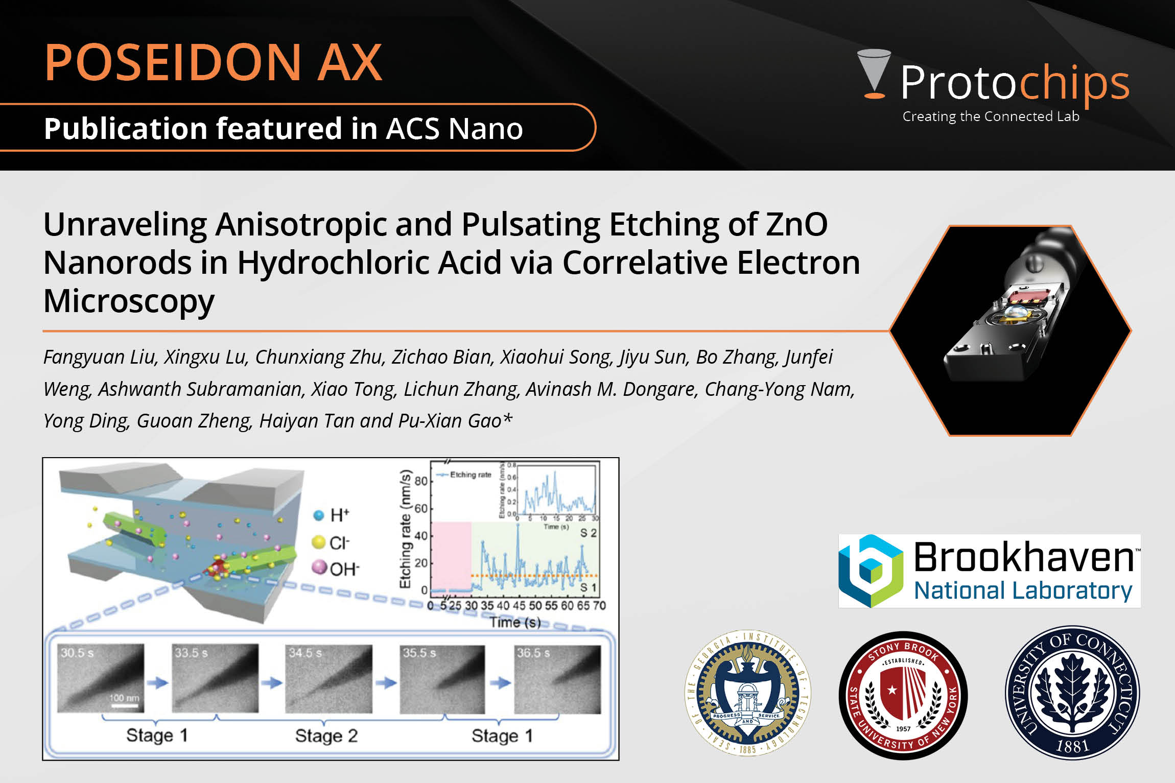
Unraveling anisotropic an...Jul. 21, 2023
What have our users done in the field? Read our summaries here!
-

Nanomaterial Synthesis One Pager
Download the one pager that shows how PoseidonAX can be used to study nanomaterial synthesis with in situ electron microscopy.
-
Radiolysis & Liquid-EM
In this application note, written by Protochips, we summarize how in situ electron microscopy using liquid phase is challenged by radiolysis side effects and how to minimize these effects.
-
Using Protochips AXON Software for Tracking Electron Flux and Cumulative Dose
In this paper, we take a look at how AXON Dose tracks the electron flux and cumulative dose, and why this might be useful for all experiments.
-
EDS and EELS analysis in the TEM using the Poseidon Liquid Cell System
This paper, written by Protochips, summarizes different publications on how to best do EELS and EDS in liquid environments.
-
Dynamic Imaging and Elemental Analysis of Nanostructures in Liquid
In this paper, written by Protochips, nanometer resolution elemental mapping of nanostructures in solution was demonstrated using the Poseidon system.
-
In Situ Few Layer Graphene Etching Using Iron Nanoparticles
In this summarized paper, researchers at DSI-IPCMS-CNRS/University of Strasbourg, (France, G. Melinte, Dr. S. Moldovan and Prof. O. Ersen) used the Atmosphere system to visualize the FLG etching process under relevant reaction conditions.
-
Atomic Scale Imaging of 2-D Materials
This paper shows how Alex Zettl’s lab at UC Berkeley and at the National Center for Electron Microscopy at Lawrence Berkeley National Laboratory (NCEM, LBNL) have characterized the atomic scale structure of CVD grown h-BN in situ in the TEM using a Fusion system.
-
Atomic Resolution Imaging at High Temperatures in the TEAM 0.5
Read how the TEAM 0.5 TEM at the National Center for Electron Microscopy (NCEM) at Lawrence Berkeley National Laboratory (LBNL) can be used to gain atomic resolution images using a Fusion system.
-
Thermal Stability Study of LAST Thermoelectric Material in the SEM
In this applications note written by Protochips, the capability of the Fusion holder was tested for the thermal and electrical properties of thermoelectric materials.
-
EDS in the TEM and SEM using Fusion
In this applications note written by Protochips, the design of the Fusion holder was tested to show full compatibility with all EDS systems.
-
Thermal Drift and Settle Times Measured for Different Temperature Excursions in the TEM
In this applications note written by Protochips, drift and settle time characteristics of Fusion, two sets of experiments were performed.
Videos
Watch dynamic behavior of real samples in situ.
Video courtesy Dr. Saso Sturm of the Jozef Stefan Institute. Acquired using the Poseidon Select liquid cell holder with liquid heating capability. More info at www.protochips.com
Electron beam induced growth of lead nanoparticles from a 40 mM aqueous solution of Pb(NO3)2. Nucleation was induced by the electron beam, and the particles grow via an Oswaldt ripening process followed by second growth stage in which the particles increase uniformly in size. The Oswaldt ripening process is indicated by the red circle. When these nanoparticles are in close proximity to larger nanoparticles, they decrease in size and ultimately disappear, while larger nanoparticles increase in size.
The movie was recorded using FEI Tecnai Biotwin operated at 120 KV and is courtesy of Dr. Albert D. Dukes, III, Lander University and Dr. Deborah Kelly, Virginia Tech.
30 nm gold nanoparticles attracted to the electron beam in a liquid thickness of 150 nm. Images collected using a Philips/FEI CM300FEG TEM at 300 kV. Courtesy of Dr. Kate Klein, National Institute of Standards and Technology. For more information on Poseidon, visit http://bit.ly/protochipsposeidon.
This real-time video shows rapid heating and quenching of micron-sized copper-silver particles in the SEM. The video demonstrates how quickly the Protochips Fusion™ can heat and quench samples, on the order of milliseconds. Take note of the temperature display on the upper left corner of the video. For more information on Fusion, visit www.protochips.com/fusion
This real-time video shows two gold nanoparticles that are on the surface of larger iron oxide particles at 900° C. At this temperature the gold is very mobile, and the two particles coalesce into one larger nanoparticle. This demonstrates the stability of the Protochips Fusion system at high temperatures. This video was taken on a JEOL ARM200F (200 kV, Cs aberration correction) at JEOL in Akishima, Japan. For more information on Fusion, visit www.protochips.com/fusion
This real time video shows rapid heating and quenching of micron-sized copper-silver particles in the SEM. The video is real time and demonstrates how quickly the Protochips Fusion™ can heat and quench samples, on the order of milliseconds. Take note of the temperature display on the upper left corner of the video.
Learn about Protochips' groundbreaking liquid cell for in situ TEM and STEM.
Experiment: Beam-Induced gold deposition from a solution of 1 mM HAuCl4 onto AuPt Nanoparticles. Heating ramp from 25 – 45 C.
#FindYourBreakthrough | FLASH TALKS: EP #7
Catalyst Particle Growth at the Nanoscale
In Situ TEM of TiO2 Supported Gold Nanoparticle Growth
Presented by: Dr. Mark J. Meijerink from Utrecht University. Read the full publication here:
https://pubs.acs.org/doi/10.1021/acs.jpcc.9b10237
#FindYourBreakthrough | FLASH TALKS: EP #8
Attachment of Iron Oxide Nanoparticles to Carbon Nanofibers Studies by In-Situ Liquid Phase Transmission Electron Microscopy
Presented by: Dr. Nynke A. Krans from Utrecht University. Read the full publication here: https://pubmed.ncbi.nlm.nih.gov/30468967/
In this Flash Talk episode 9 Joanna Korpanty from Northwestern University, Department of Chemistry will tell you something about her recent publication on solvated polymeric nanomaterials in liquid cell electron microscopy. A worm-to-micelle transformation was triggered via organic solvent mixing during the measurements, showing dynamics not possible with cryo-electron microscopy. This work shows great potential in future liquid cell experiments in other solvents then water.
Full publication:
https://linkinghub.elsevier.com/retrieve/pii/S266638642200039X
#FindYourBreakthrough | FLASH TALKS: EP #17
High-Entropy-Alloy Nanocrystal Based Macro- and Mesoporous Materials
In this flash talk, a soft-chemistry route to fabricate ordered macro- and mesoporous materials based on high-entropy alloy nanoparticles is introduced. In situ electron microscopy is used to observe the stability of these newly formed nanoparticles under atmosphere.
Presented by: Dr. Maria de Marco from the Laboratoire de Chimie de la Matière Condensée de Paris (LCMCP) and the Institut de Physique et Chimie de Matériaux de Strasbourg (IPCMS). Read the full publication here:
https://pubs.acs.org/doi/10.1021/acsnano.2c05465
Products featured: Protochips AtmosphereAX