

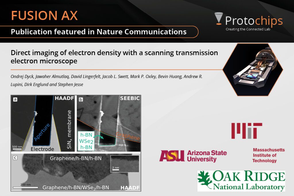
Tuesday publication update! A new pioneering technique, known as secondary electron e-beam-induced current (SEEBIC), offers atomic-scale insights into material properties like conductivity, connectivity, and work function. However, this technique can also be used together with in situ electron microscopy. In this newest work, authors used the #FusionAX system and SEEBIC imaging on a stacked 2D heterostructure device, unveiling the spatial electron density of an encapsulated WSe2 layer.
Surprisingly, the double Se lattice site exhibited higher emission compared to the W site, challenging existing valence ionization models of isolated WSe2 clusters.
These findings shed light on the potential for atomic-level SEEBIC contrast within a single material, signaling the need for a deeper understanding of atomic-scale SE emission. This quest promises insights into interlayer bonding nuances and their impact on electron orbitals, offering a glimpse into future possibilities for this technique.
Want to read the entire work?
Find it here!
https://www.doi.org/10.1038/s41467-023-42256-9
#Findyourbreakthrough #nanomaterials #SEEBIC #insituelectronmicroscopy #protochips


