Come Find Us at PICO 2024 in the Netherlands!
April 19, 2024


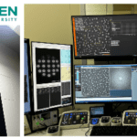
New FIB-optimized E-chips use the same sample preparation procedures you are used to in traditional FIB preparation and produce better electrical measurements. (Left) Create thin lamellae liftouts and attach them to E-chips with ease and (middle) conduct final thinning directly on the E-chip without damaging the E-chip contacts or electrical leads. (Right) Electrical profile of a Conductive Bridge Resistive Memory (CBRAM) device tested with FIB-optimized E-chips.
Using the same steps as traditional FIB sample preparation, these E-chips enable anyone to create high-quality, thin lamellae for in situ electrical biasing experiments. Prepare samples in ½ the time by eliminating extra steps necessary for FIB preparation on normal E-chips.
Conduct 4-point probe or 2-point probe measurements on your sample using the E-chip configuration that’s right for you. Available in two unique configurations, the FIB-optimized E-chips are ideally suited for studying materials ranging from p-n junctions, CMOS devices, resistive memory devices, piezoelectrics, and much more.


Customize your experiment with either the 2-point (left) or 4-point probe (right) configurations of these new E-chips
Maximize the quality of your experiment by eliminating beam damage to your sample and the E-chip contacts. Because of the unique notched design, samples can be welded to electrical leads and thinned to electron transparency without affecting electrical contacts.
Want more information? Send your questions to orders@protochips.com today!